Model Frame Buffer Interface
Various video processing applications require storing a full frame of video. For instance, some algorithms compute data across an entire video frame, then use the computed data to modify the current frame. The algorithm must store the current video frame during computations. Other uses of frame buffers include frame rate conversion algorithms, or forming a contiguous video stream from bursty data.
This support package provides a simplified simulation model of a frame buffer, and provides interfaces on the FPGA reference design that connect to external memory on the board. The reference design implements the frame buffer interface using two-channel AXI4-Stream video direct memory access (VDMA).
Note
The frame buffer external memory interface is not supported with multipixel streaming or when using a MIPI® FMC card.
The frame buffer interface uses the streaming video control signals from Vision HDL Toolbox™. The buffer stores one frame and returns the frame when requested. You can write a second frame to the buffer while reading the previously stored frame. The buffer recreates the streaming video control signals for the output frame.
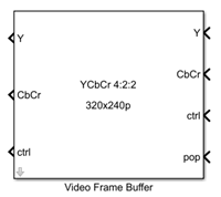
To model a frame buffer interface, start your design using one of the Pixel-Streaming Design with Frame Buffer template models. See Create Model Using Simulink Templates. The template includes a subsystem that models the frame buffer interface.
You can select the color space and frame size on the subsystem mask. The subsystem handles video control signals, address generation, and pixel data packing and unpacking. The subsystem does not simulate the physical memory bus protocol, timing, or contention.

The frame buffer returns the stored frame when it receives a pop request signal. The pop request should occur only once per frame.
The buffer reuses the input frame control signals for the output frame. At a pop request, the buffer returns the frame data starting at the next input ctrl.vStart signal. Therefore, if you pop the buffer in the blanking period at the end of the written frame, the latency is less than one frame as shown in the waveform. The top three signals are the output of the frame buffer. The bottom four signals are the input to the frame buffer, from the FPGA-targeted subsystem in the Histogram Equalization with Zynq-Based Hardware example. The bottom signal is the pop request.

If you pop the buffer after the next frame has started writing, the output frame is delayed until the next ctrl.vStart, as shown in this waveform.

Alternatively, you can copy the Video Frame Buffer subsystem found in both the Histogram Equalization with Zynq-Based Hardware and Lane Detection with Zynq-Based Hardware examples. Connect this subsystem to your FPGA-targeted subsystem.
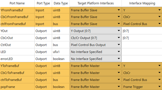
For deployment to FPGA, map the frame buffer interface ports of your FPGA user logic to the frame buffer interface in the reference design. At step 1.3 in HDL Workflow Advisor, select the Frame Buffer Master and Frame Buffer Slave interfaces, as shown.

The reference design reserves 64Mb of address space for the frame buffer, and assigns a fixed address offset. The device tree of the board operating system ensures other processes cannot access the same memory space.
