Image Rotation with Zynq-Based Hardware
This example shows how to target an image rotation algorithm to the Zynq® hardware by using the IP core generation workflow of the SoC Blockset™ Support Package for AMD® FPGA and SoC Devices. This example also shows a memory performance analysis of the image rotation algorithm from the hardware.
Setup Prerequisites
This example follows the algorithm development workflow that is detailed in the Developing Vision Algorithms for Zynq-Based Hardware example. If you have not already done so, work through that example to gain better understanding of the required workflow.
The algorithm works on a 720p HDTV (1280x720) video source, selects a square 500x500 pixel Region of Interest (ROI) of the central portion of the 720p video stream, and performs a 90 degree clockwise rotation of the ROI.
If you have not yet done so, run through the guided setup wizard portion of the Zynq support package installation. You might have already completed this step when you installed this support package.
On the MATLAB® Home tab, in the Environment section of the Toolstrip, click Add-Ons > Manage Add-Ons. Locate SoC Blockset Support Package for AMD FPGA and SoC Devices, and click Setup.
The guided setup wizard performs a number of initial setup steps, and confirms that the target can boot and that the host and target can communicate.
For more information, see Set Up Xilinx Devices.
Pixel-Stream Model
This example uses the simplified AXI4 Master protocol to interface with external memory. For more information, see Model Design for AXI4 Master Interface Generation (HDL Coder).
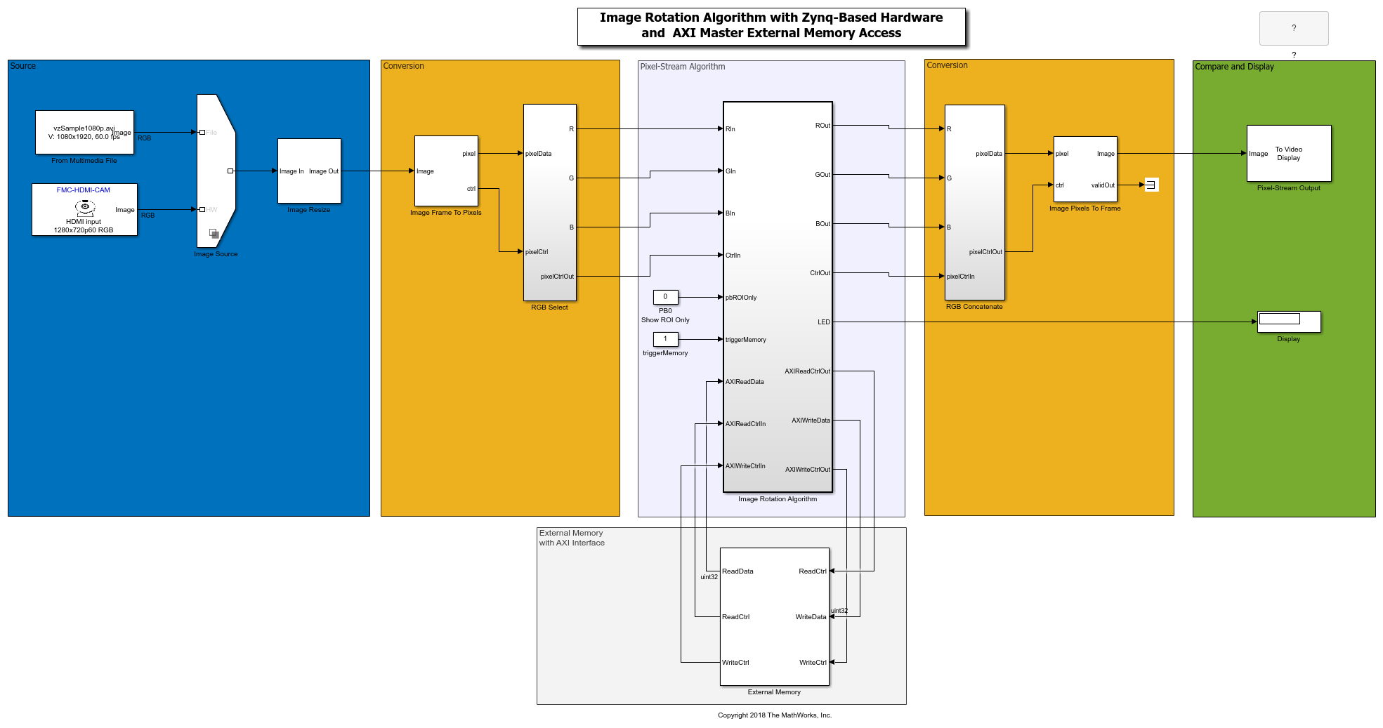
This model uses a Image Resize block that allows the source video frame to be resized for better simulation performance. Alternatively, you may want to perform a crop of the video frame. The blocks in the shaded areas convert to and from pixel stream signals in preparation for targeting.
The algorithm in this example performs image rotation on a central region of an input video stream. The central region of the stream is selected by specifying a Region of Interest (ROI). The image rotation is performed by transferring the output of the ROI to external memory in bursts of rows, before individual pixels are read back from external memory in columns.
open_system('vzImageRotation_PixelStream')

Video Source The source video for this example comes from either the From Multimedia File block, that reads video data from a multimedia file, or from the Video Capture HDMI block, that captures live video frames from an HDMI source connected to the Zynq-based hardware. To configure the source, right-click on the variant selection icon in the lower-left corner of the Image Source block, choose Label mode active choice, and select either File or HW.
For this algorithm, the model is configured as listed:
A pixel format of RGB. This algorithm is written to work on a RGB pixel format, and both the From Multimedia File and Video Capture blocks are configured to deliver video frames in this format. Other supported pixel formats are YCbCr 4:2:2, and Y only.
Algorithm Configuration The algorithm, in addition to processing the image for image rotation has some control as well.
pbROIOnlyconnects to a push button on the board to display the output of the ROI selection, without image rotation applied.
The pbROIOnly control port is a pure hardware connection in the targeted design. This port can run at any desired rate including at the pixel clock rate.
The triggerMemory port enables memory access. Data is written to or read from DDR memory only when this signal is 1. This enable signal prevents memory accesses starting as soon as the bitstream is loaded.
The model features an External Memory block that provides a simplified simulation model of an external memory interface. In the targeted design, the bus connections will interface with the external memory on the chosen Zynq platform.
The External Memory block port interface can be separated into two channels that correspond to the simplified AXI4 Master protocol: Write Channel and Read Channel.
The Write Channel interface is comprised of the scalar WriteData input port, and the WriteCtrl input and output bus ports. The WriteData input port is for the data values that are to be written to external memory. The WriteCtrl bus port contains the bussed write request signals { wr_addr, wr_len, wr_valid} that specify the destination address, burst length, and validity of the data being written to memory. The WriteCtrl output port returns the bussed write response signals { wr_ready, wr_complete} that specify the readiness of the external memory to accept data, and to signal that a write transaction has completed successfully.
For more information on the Write Channel, see Simplified AXI4 Master Protocol - Write Channel (HDL Coder).
The ReadChannel interface is comprised of the ReadData scalar output port, and the ReadCtrl input and output bus ports. The ReadData output port is for the data values that are being read from external memory. The ReadCtrl input bus port contains the bussed read request signals { rd_addr, rd_len, rd_avalid, rd_dready} that specify the start address, burst length, validity of the read address, and the readyness of the DUT to accept read data. The ReadCtrl output bus port contains the bussed read response signals { rd_aready, rd_dvalid} that specify the response from the external memory that the memory interface can accept read requests, and the validity of the returned read data.
For more information on the Read Channel, see Simplified AXI4 Master Protocol - Read Channel (HDL Coder).
NOTE: During the first frame of simulation output, the Video Display scope display a black image. This condition indicates that no image data is available. This behavior is because the output of the pixel-streaming algorithm must be buffered to form a full-frame before being displayed.
Image Rotation Algorithm
The image rotation algorithm is shown below.
![]()
The Image Rotation Algorithm subsystem contains the following components:
ROI Selector blocks: Selects the central region of the input video stream. One ROI Selector block for each of the three RGB video components.
ToMemory: Writes the central ROI image stream to external memory in bursts of length equivalent to the horizontal (row) size of the ROI.
FromMemory: Performs the image rotation operation by reading the ROI pixel data back from external memory in bursts of single pixels. The rotation is performed by reading the pixel data in columns starting from the bottom row. This performs a 90 degree clockwise rotation of the ROI.
Selector: Selects if the original ROI image, or the rotated image, is shown on the HDMI output. The selection is determined by the pressing of a push button in the targeted hardware design.
Target the Algorithm
After you are satisfied with the pixel streaming algorithm simulation, you can target the pixel algorithm to the FPGA on the Zynq board.
Start the targeting workflow by right clicking the Image Rotation Algorithm subsystem and selecting HDL Code > HDL Workflow Advisor.
In Step 1.1, select
IP Core Generationworkflow and select your target platform from the list.In Step 1.2, select
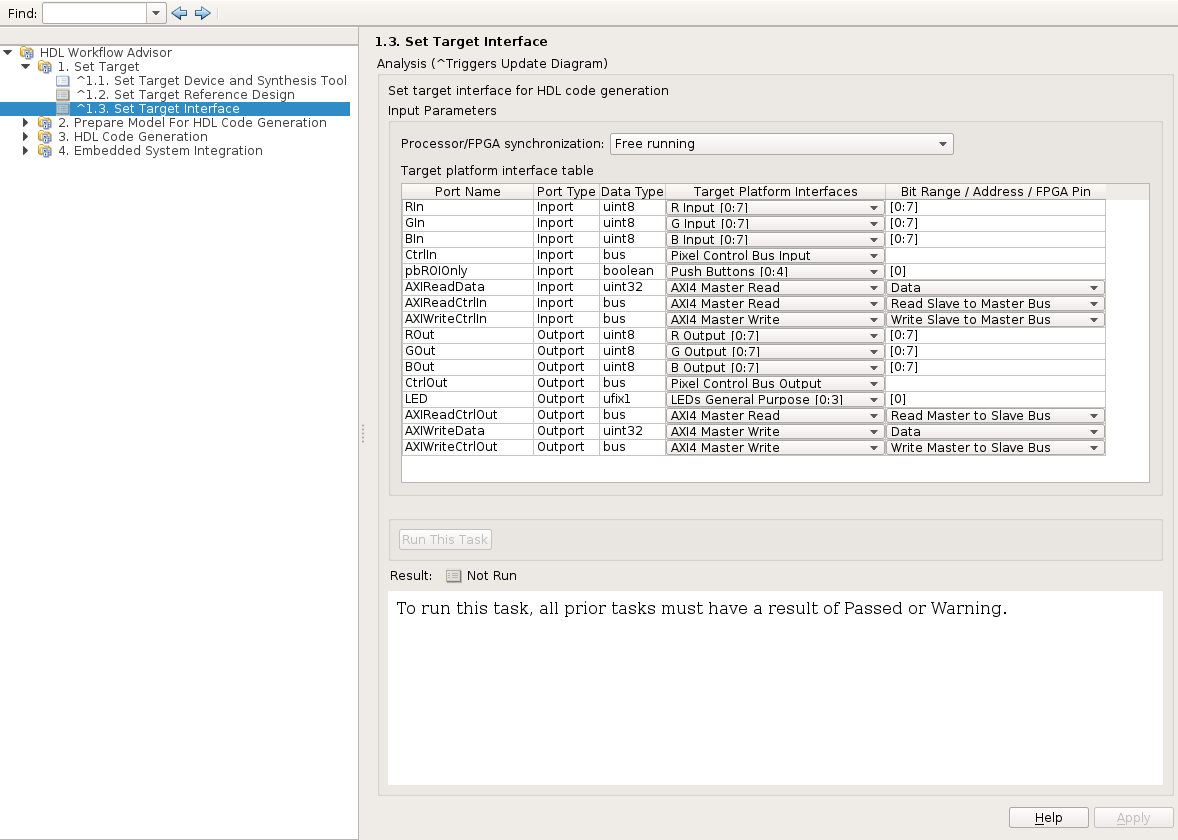
RGBreference design to match the pixel format of the Image Rotation Algorithm subsystem, and select720p HDTV (1280x720p)as the source video resolution.In Step 1.3, map the target platform interfaces to the input and output ports of your design. As this example uses the frame buffer interface, the relevant ports of the Image Rotation Algorithm subsystem must be mapped accordingly.
The Read Channel of the AXI4 Master interface will be mapped to the AXI4 Master Read interface, and the Write Channel of the AXI4 Master interface will be mapped to the AXI4 Master Write interface.
With reference to Target platform interface table, map the AXIReadData port to the AXI4 Master Read interface, and select Data from the dropdown menu in the Bit Range / Address / FPGA Pin column. Similarly, select AXI4 Master Read as the interface for the AXIReadCtrlIn and AXIReadCtrlOut ports, and Read Slave to Master Bus and Read Master to Slave Bus from the Bit Range / Address / FPGA Pin column respectively.
Map the AXIWriteData, AXIWriteCtrlIn, and AXIWriteCtrlOut ports to the AXI4 Master Write interface, and select Data, Write Slave to Master Bus, and Write Master to Slave Bus from the dropdown menu in the Bit Range / Address / FPGA Pin column respectively.

Additionally, map the pbROIOnly port to push button 0, and the LED port to LED 0.
Step 2 prepares the design for generation by doing some design checks.
Step 3 generates HDL code for the IP core.
Step 4 integrates the newly generated IP core into the larger Vision Zynq reference design.
Execute each step in sequence to experience the full workflow, or, if you are already familiar with preparation and HDL code generation phases, right-click Step 4.1 in the table of contents on the left hand side and select Run to selected task.
In Step 4.2, the workflow generates a targeted hardware interface model and, if the Embedded Coder® Support Package for AMD SoC Devices has been installed, a Zynq software interface model. Click
Run this taskbutton with the default settings.
Steps 4.3 and 4.4
The rest of the workflow generates a bitstream for the FPGA, downloads it to the target, and reboots the board.
Because this process can take 20-40 minutes, you can choose to bypass this step by using a pre-generated bitstream for this example that ships with product and was placed on the SDCard during setup.
Note: This bitstream was generated with the HDMI pixel clock constrained to 74.25 MHz for a maximum resolution of 720p HDTV at 60 frames-per-second. To run this example on Zynq hardware with a higher resolution, select the Source Video Resolution value from the drop-down list in Step 1.2.
To use this pre-generated bitstream execute the following:
>> vz = visionzynq();
>> changeFPGAImage(vz,'visionzynq-picozed-hdmicam-image_rotation.bit');
To use a bitstream for another platform, replace 'picozed' with the platform name. When you target this example to ZCU102 or ZCU106 board, the design uses PL DDR memory.
Alternatively, you can continue with Steps 4.3 and 4.4.
Using the Generated Models from the HDL Workflow Advisor
Step 4.2 generated two, or four, models depending on whether Embedded Coder® is installed: A 'targeted hardware interface' model and associated library model, and a 'software interface' model and associated library model. The 'targeted hardware interface' model can be used to control the reference design from the Simulink model without Embedded Coder. The 'software interface' model supports full software targeting to the Zynq when Embedded Coder and the Embedded Coder® Support Package for AMD SoC Devices are installed, enabling External mode simulation, Processor-in-the-loop, and full deployment.
The library models are created so that any changes to the hardware generation model are propagated to any custom targeted hardware simulation or software interface models that exist.
Targeted Hardware Interface Model: In this model, you can adjust the configuration of the reference design and read or drive control ports of the hardware user logic. These configuration changes affect the design while it is running on the target. You can also display captured video from the target device.
Software Interface Model: In this model, you can run in External mode to control the configuration of the reference design, and read or drive any control ports of the hardware user logic that you connected to AXI-Lite registers. These configuration changes affect the design while it is running on the target. You can use this model to fully deploy a software design. (This model is generated only if Embedded Coder and the Embedded Coder Support Package for AMD SoC Devices are installed.)
Memory Analysis of Image Rotation
SoC Blockset provides AXI performance monitor (APM) to get the memory diagnostics from the hardware. To get the memory diagnostics information for the image rotation DUT while accessing the external DDR4 memory, add the APM IP between the DUT and external DDR4 memory.
In Step 1.2 of HDL Workflow Advisor, select
RGB with APMreference design to get the memory performance while writing and reading from the external DDR memory.Follow all the HDL Workflow Advisor above steps to generate the bitstream and deploy it on to the hardware.
Run the host model or software interface model mentioned in above steps to see the inverted image.
Run the
vzWithAPM_aximanager.mscript from the current project folder.Once performance plots view is open, to see the bandwidth, bursts and latencies of each master, select the corresponding master and click Update.
The image rotation algorithm in this example selects a square 500x500 pixel region of interest (ROI) of the video stream, and performs a 90 degree clockwise rotation of the ROI. So, algorithm writes and reads from external DDR4 memory only 500x500 pixel region. The bandwidth requirement for the image rotation algorithm with frame rate of 60 FPS to write and read from the external memory is calculated as:
Image size = 500x500
Video format = RGB
Number of bytes in each pixel = 3
Video frame rate = 60 FPS
Zero padded bytes = 1
Total required bandwidth = 500x500x4x60 = 60 MBPS
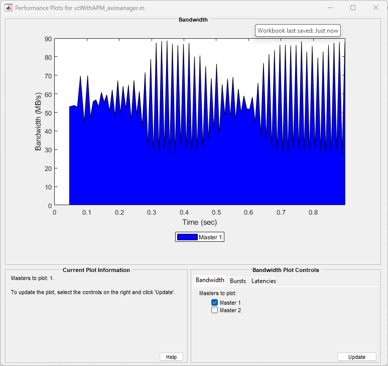
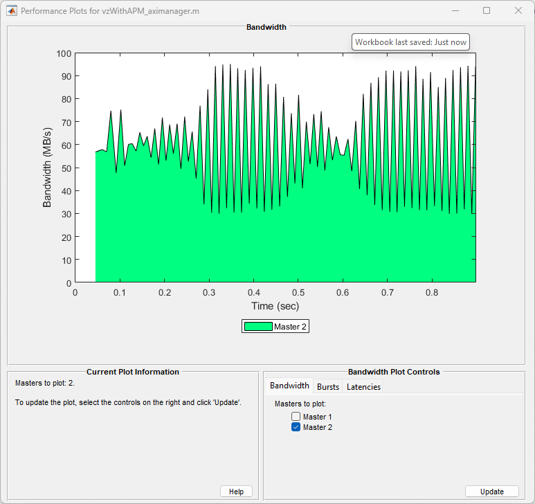
You can see the average bandwidth from the below plots for writing into the external DDR4 memory and reading from the memory. In the plots master1 is for write and master2 is for read.
Bandwidth plots for read and write masters.


Similarly, you can plot the number of bursts and latencies for write and read masters by selecting them correspondingly in the performance plots (not shown).
